- Time:2025-09-11
- Venue:2C, 2nd Floor, Hall 2
- Language:CN
Organizer
China International Optoelectronic Exposition
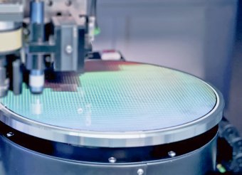
Laser technology with high precision, non-contact, high efficiency and other advantages, positive depth of the enabling semiconductor industry chain upgrade, covering integrated circuits, display panels, photovoltaic, semiconductor lighting and other fields. In chip manufacturing, extreme ultraviolet (EUV) laser lithography technology breaks through the process bottleneck below 7nm, supporting the development of 5G/AI chips; Excimer laser annealing (ELA) helps OLED panel low-temperature polysilicon film preparation to improve the display resolution; Ultrafast laser (femtosecond/picosecond) is applied to Mini/Micro LED chip cutting, and the yield is increased to 99.9%. In addition, laser-induced breakdown spectroscopy (LIBS) enables online wafer defect detection, fiber laser welding technology ensures the reliability of IGBT module packaging, and silicon carbide substrate laser stripping technology also promotes the cost reduction and efficiency increase of third-generation semiconductors.
The "Laser Technology Enabling Semiconductor Industry Manufacturing Forum" aims to bring together experts and scholars, enterprise representatives and industry elites in the field of laser technology and pan-semiconductor industry, jointly focus on the collaborative innovation of laser technology and pan-semiconductor manufacturing, and promote the technological research and ecological construction of the industrial chain.