- Time:2025-09-11
- Venue:5C, 2nd Floor, Hall 5
- Language:CN
Organizer
Hong Kong Applied Science and Technology Research Institute
Shenzhen UBM Herong Exhibition Co., Ltd
China International Optoelectronic Exposition
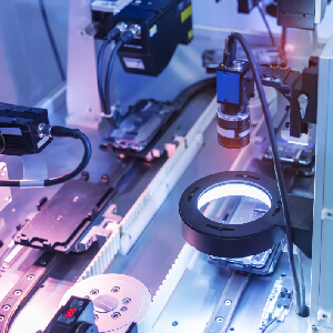
As the semiconductor industry moves towards the "post-Moore era", semiconductor inspection technology is undergoing profound changes. As the critical dimensions of integrated circuit packaging processes continue to be reduced and the packaging become 3D IC, the pressure of the production yield has increased dramatically, making the inspection technology become the key to control the overall industrial development. Compared with traditional visual inspection equipment, semiconductor inspection equipment not only relies on many complex optical technologies, which become extremely high technical barriers, but also requires a large amount of capital investment and a long investment return cycle. More importantly, the domestic substitution rate of equipment has become a bottleneck restricting the development of the entire national industry. Against the backdrop of increasingly fierce competition in the global semiconductor industry, China's semiconductor industries will keep accelerating the process of domestic substitution, increasing R&D investment, enhance technological innovation capabilities, and continuously narrowing the gaps between with international advanced levels. At the same time, the construction of the industrial ecology will be further strengthened, and through close cooperation between industries, academia, research and user, the semiconductor machine vision industry chain will be further improved to enhance the overall competitiveness of the national industry.
This forum will invite top companies such as Jingce Electronics, Motic, Suzhou Vega, ZEIT etc. to share their latest technologies in semiconductor 2D/3D inspection, computational imaging, critical dimension metrologies for semiconductor in front-end and mid-end advanced packaging, to accelerate the development of national semiconductor industries.